Since the 1947 invention of the transistor by three Bell Labs scientists and their subsequent winning of the 1956 Nobel Prize, technology has been rolling on.
Dubbed a development “that changed the world,” the existence of this key, little machine has led to a technological and device revolution. It is the central reason we can all walk around every day with all the computing power in our pockets that used to fit in a humongous supercomputer installation.
Talk about the Information Revolution. We’ve got the entirety of man’s knowledge at our fingertips.
For those not up on precisely what a transistor is, here’s a simple explanation: “A transistor is a semiconductor device used to amplify or switch electronic signals and electrical power. It is composed of semiconductor material usually with at least three terminals for connection to an external circuit. The transistor is the fundamental building block of modern electronic devices, and is ubiquitous in modern electronic systems. ”
And the evolution of Moore’s Law (loosely, the number of transistors doubles every year while their price is cut in half) has continued, unbelievably.
Gordon Moore (co-founder of Fairchild Semiconductor and Intel) predicted in 1965 that this would reliably occur and in 1975 because semiconductors were getting so small, revised his law to the doubling occurring every two years.
This prescient man’s vision somehow saw the future and made a law out of the business that propels technology farther and farther.
“This powerful technology has allowed us to make more and more complex and high-performing circuits ... They’re the basis of everything electronic we have, unprecedented in human history.” -Gordon Moore (1929-present)
But nobody ever thought Moore’s Law could go on forever: after all, getting more inexpensive meant someday being free and getting smaller and smaller should be impossible once certain smallness is achieved.
Now, it is in the spirit of technological advancement that the University of California Berkeley and their Berkeley Labs recently announced that a team of scientists, researchers, post-doctoral and graduate students have invented the world’s smallest transistor.
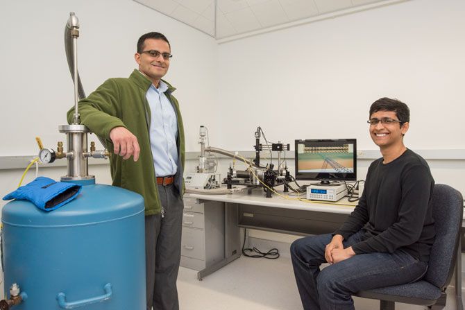
Ali Javey, professor of Electrical Engineering & Computer Science and Berkeley and his graduate student studying for his Ph.D., Sujay Desai have spent the last two years conceptualizing, finding funding, researching, discovering and finally, building this new infinitesimally small “experimental device.”

But talk about a team effort: Lawrence Berkeley National Laboratory and UC Berkeley led the project with primary funding coming from the US Department of Energy with strong contributions by Stanford University and the University of Texas Dallas.
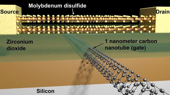
According to the recent press release, “Transistors consist of three terminals: a source, a drain, and a gate. Current flows from the source to the drain, and that flow is controlled by the gate, which switches on and off in response to the voltage applied.”
It is the gate that must get smaller and smaller to allow for miniaturization. The release added, “For more than a decade, engineers have been eyeing the finish line in the race to shrink the size of components in integrated circuits. They knew that the laws of physics had set a 5-nanometer threshold on the size of transistor gates among conventional semiconductors, about one-quarter the size of high-end, 20-nanometer-gate transistors now on the market.”
How small is the gate on this new transistor?
This new gate is a previously thought impossible, one-nanometer thick.
Perspective? A human hair is 50,000 nanometers. So the gate is one-50,000th the size of a human hair.
Using a new ingredient in transistor development: Molybdenum disulfide or “MoS2,” the research team happened upon the engine lubricant in powder form present in some fairly typical households, that in solid form allowed for the creation of this smaller gate in the transistor.
"The semiconductor industry has long assumed that any gate below 5 nanometers wouldn’t work, so anything below that was not even considered," said study lead author Sujay Desai, a graduate student in Javey's lab. "This research shows that sub-5-nanometer gates should not be discounted. Industry has been squeezing every last bit of capability out of silicon. By changing the material from silicon to MoS2, we can make a transistor with a gate that is just 1 nanometer in length, and operate it like a switch."

“Molly Sulfide” as Professor Ali Javey calls MOS2, seemed to be the key breakthrough. “We started the project about two years ago, when Sujay (Desai) and I came up with the idea. About ten people worked on our team,” Professor Javey told me. “The students and post-docs worked on making the batches of first functioning devices in Berkeley’s 100/1000 class clean room where we did the fabrication. We got the carbon nanotubes from Stanford.”

Javey said the team had the first functioning devices within six months of the project’s start, and then finished honing and refining the devices six months ago. They then submitted their paper—which is the final step in any invention of this kind—six months ago. So 18 months in total yielded this impressive development.
Meanwhile, the team carries on. According to Javey, they “have obtained some provisional patents on the materials aspects of the experimental device and are exploring other patents.” I’ll just bet they are, I thought as I wondered how long it might take an Intel or AMD to come knocking on their door.
It is precisely these kinds of PPP (Public-Private Partnerships) where government works with academia’s bright young minds, that a panoply of the world’s progress is realized.
Without this innovation-engine dynamic, we wouldn’t have the Internet itself or untold other inventions, medicines and life-saving technologies. Not to mention creature comforts.
